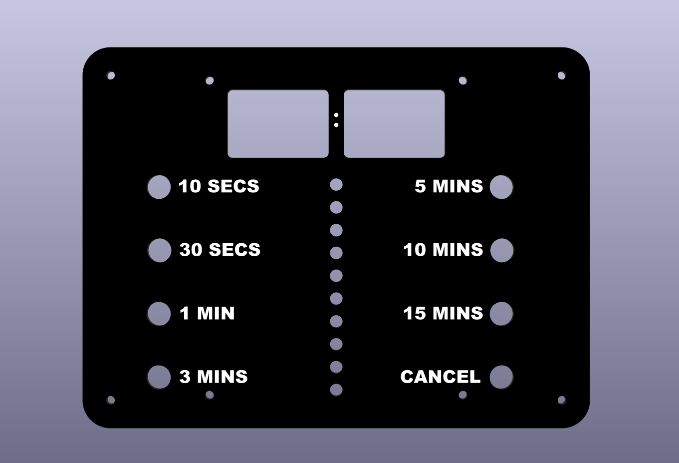
The idea for this project was a simple countdown timer to be used by children for various games and activities where the user interface was designed to be as simple as possible; the display was clear from across the room and provided a sense of urgency, with a clear notification when the time was up. I started from the need for a large bright display, which meant using the largest economically available 7-segment LED modules. Starting a timer should be as simple as pressing a single button with a fixed function, so there is no time adjustment (up/down) facility which can be fiddly and non-obvious to use. Those often require long presses to get into a fast increment mode and are not consistent in how they accelerate. Choosing the time periods at the start of the project meant that the front panel could be labelled. Seven periods covered the desired range of 10 seconds to 15 minutes and left one button to be used for cancel, making a nicely symmetrical 4 buttons arrangement down either side. A coloured bargraph display was designed to give a sense of what proportion of the original time has elapsed and how much remains, using 10% steps. A speaker was included to play a tune when the countdown was completed.
PCB Design Tools
CAD packages for PCB design have seen
a lot of changes over the years, from clunky
DOS-based tools, through
steep-learning-curve GUIs to
expensive fully featured packages. Fortunately, in the last few years the FOSS tool
KiCad (
pronounced "key-cad"), now at version 9, has become mature and sufficiently featured and supported to be a fantastic first choice for PCB design. Additionally, low cost far-eastern manufacturers can now make the bare boards and do assembly for less cost than we used to pay just for
NRE, and deliver in less time.
PCB Size
PCB design gets harder as the design gets more cramped with components, resulting in more compromises, more vias and the need for more layers. Beginners often forget that you can't just size the board based on the component outlines, the tracks take up space too. Space also needs to be allowed for assembly processes and debugging such as attaching programming connectors and probes. An initial layout based on the chosen
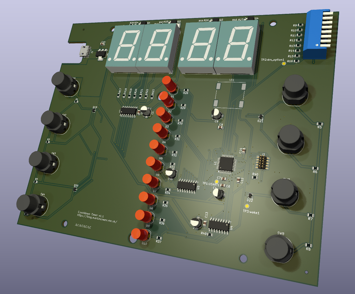
0.8" 7-segment displays, the
C&K D6R buttons and the discrete LED bargraph suggested a minimum PCB size of 150 x 150 mm. It clearly needed a backbox to prevent fingers from being cut by the sharp ends of through-hole pins and solder spikes so the board was designed to fit the
Hammond RL6655.
The maximum size of the PCB was 165 x 135 mm to fit within the front panel area.
Front Panel
Although the box comes with a front panel, it would have been beyond my mechanical skills to cut out the rectangles for the display and the holes for the buttons all aligned accurately. Labelling is very difficult to get correctly aligned and we are very sensitive to small mistakes in presentation. I'd seen
others suggest the use of a
second PCB as a front panel, using black solder mask and white silkscreen. Using the PCB manufacturer to make the front panel is a brilliant idea because they are already set up to drill accurately in precisely defined locations. It's easy to use the same PCB software as you are already using to define the cutouts and check that they align with the PCB. Aligning the mounting holes with the box was a matter of reading from the box drawing and double-checking.
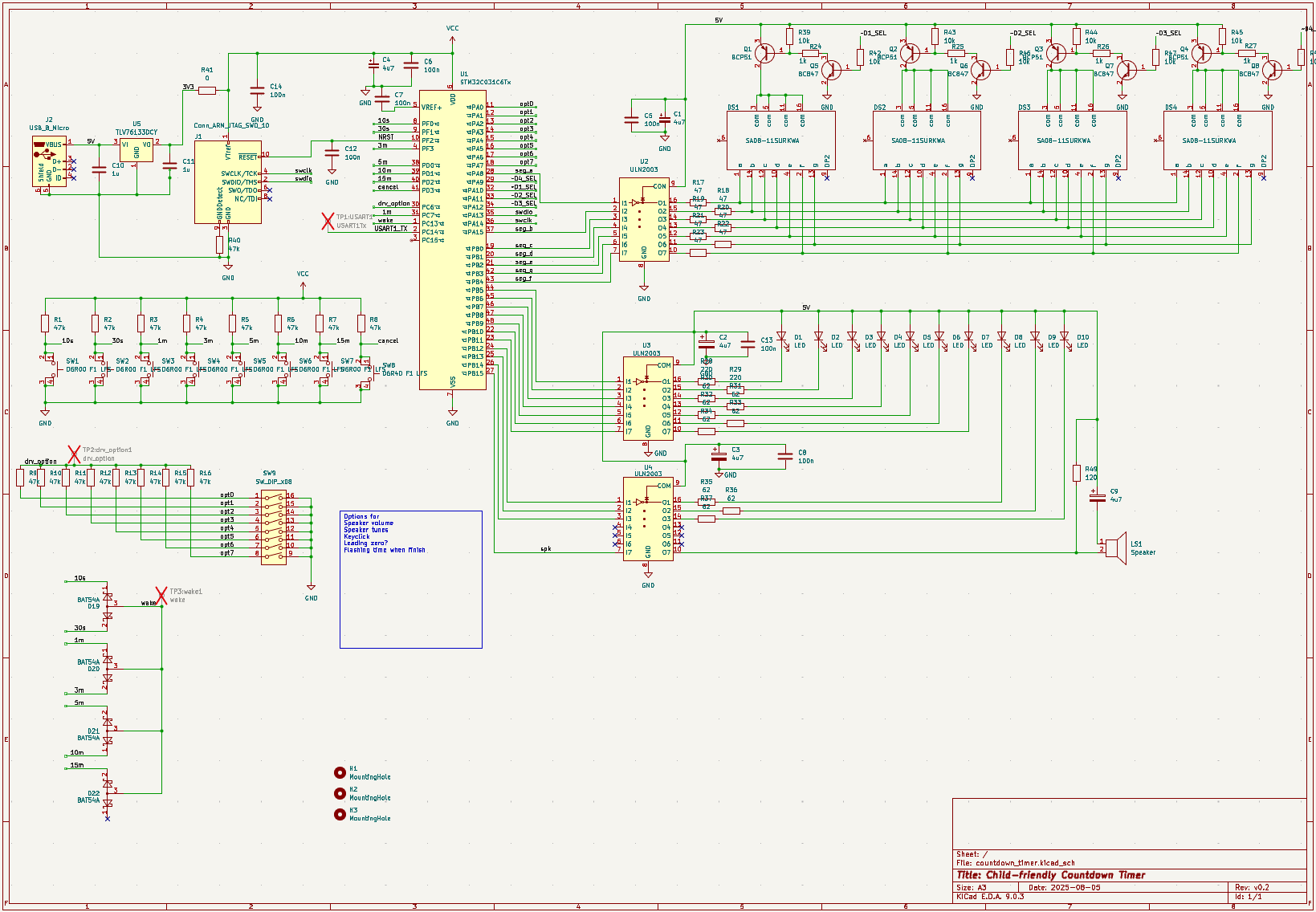
Logic
There are lots of ways of implementing the required functionality, from hardwired discrete gates through gate arrays and ROMs to microcontrollers and microprocessors with external memory. I chose to use an STM32 at the budget end of the range to see how capable these are compared to the dual-core Cortex M7+M4 480 MHz heavyweights that I'd been using recently at work. The cheapest M0+ with at least 38 IO pins that were needed for all the buttons and LEDs was the
STM32C031C6 ($0.93 Qty 1, at LCSC), which had an easily available
dev kit (£13) and comes with a STLINK-V3MINIE programmer. Additionally, the STM32C031C6 was in-stock at
LCSC. This micro has 45 IOs, 32kB flash, 12kB RAM, an internal 48 MHz 1% oscillator in a LQFP-48 package and has many useful peripherals like PWM, ADC and UART.
Programming Header
There is sufficient space between the boards using 10mm spacers for the ST Link ribbon cable to be plugged in.
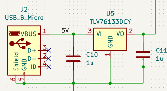
Power Supply
The original plan was to use a battery holder with 2 or 3 AA batteries, soldered to the back of the board low down to provide mechanical stability when upright. However, the power consumption of the LEDs meant that battery life was going to be very short and it was going to be more efficient to run from 5V over USB from a battery bank that I had available. The higher power components pull from the 5V line so that they don't pull current through the 3.3V regulator and heat it up. I placed a zero ohm link after the regulator which, by removing it before the board was powered up, allowed me to test the regulator on it's own without risking the processor.
When the timer has completed, the micro can go into a low current sleep mode to avoid draining the battery, but we also have to use a low quiescent, low dropout linear regulator so that this does not become a cause of a flat battery bank. The
TLV76133 draws 60uA quiescent, is rated for up to 1A and is an SMT SOT-223 package.
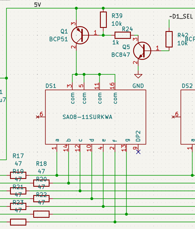
LED Drive
If you're used to PIC16/18s which can sink 20mA, you might not realise that you need to add an external sink circuit for most micros to drive LEDs, but I remembered using PIC24s that surprised us by only being 4mA capable so I planned for this potential problem by using ULN2003. Whilst they are overkill for this situation, it is less work to layout and assemble a few SOIC-16 packages than a set of 18 discrete transistor circuits.
Unfortunately the larger 1 inch 7-segment displays seemed to be common cathode only which would have meant using high side drives and I wanted to stick with ULN2003 low side drives, which don't have a high side version. This limited me to using the 0.8 inch SA08-11SURKWA displays but they are sufficiently large for this project, and turned out to be sufficient bright even when multiplexed and through an optical filter.
Each digit's common anode needed to be pulled up to the 5V rail using a PNP transistor which is turned off by a resistor between the base the rail, and needed to have it's base pulled down by an NPN.
Peak current with 47 R series resistors was measured as 43mA for 4ms, which averages to 11mA continuous equivalent, so this is within spec of 30mA continuous, peaking to 185mA for 0.1ms, .
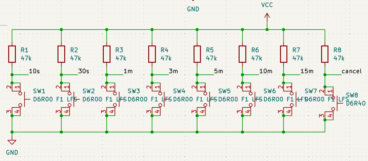
Button Detection
The button detection circuit uses pull-up resistors, with no current being drawn in the normally open state. Debouncing can be done entirely in software, although if this was a production circuit I would use some filtering on the inputs for EMC reasons. I wanted to keep to a minimal component count for this project to reduce the potential for problems, as well as for cost.
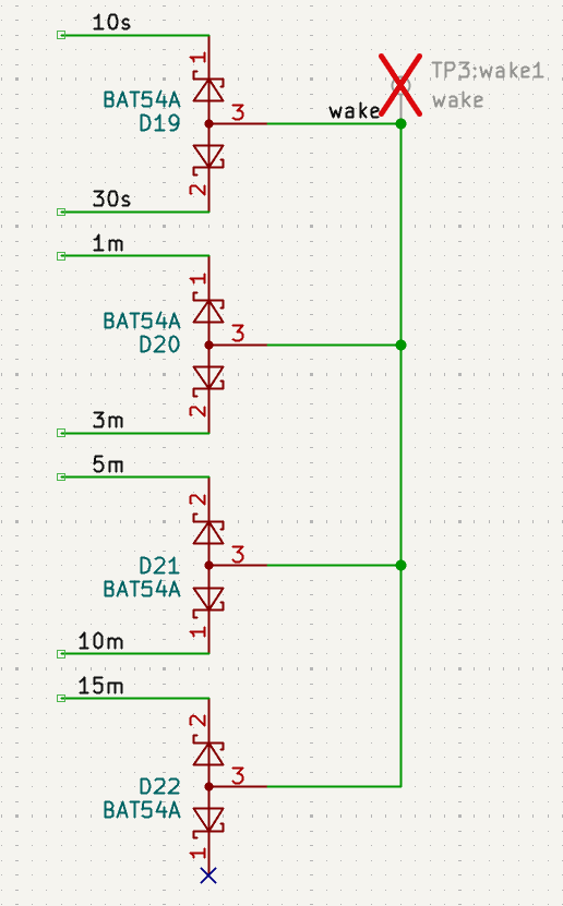
To allow for any time selection button (not including Cancel) to wake the processor from sleep, the lines are dioded together with BAT54A's and an internal pullup. If any button is pressed, the wake line will go low. These didn't need to be Schottky diodes, just cheap, in-stock, common anode diodes in a SOT-23/SOT-323 package.
Options
An 8-way DIP switch was added to provide some user-selectable options without having to change and reflash the firmware. The pullups go to a GPIO instead of the 3.3V rail so that it can be activated only when reading the switches to prevent drawing current continuously from all the on switches.
Speaker
A pull-up was necessary because the UNL2003 is open collector, and a d.c. blocking capacitor is present to avoid burning out the speaker in case of the driver being left in the on state for more than a few milliseconds. During board bring-up, IO pins may not yet be setup correctly and even after they have been, halting the program at a random location could leave a pin driven for longer than they would whilst running. The speaker is driven from PB15 which has a PWM peripheral option using channel 3N, enabling uninterrupted tones without interrupting the micro at the tone frequency.
Schematic
Board Design
Mechanical Considerations
The height of the displays and buttons meant that
10mm spacers were ideal for placing the front panel at the right height. Four suitable locations were found for these spacers and
black-headed M3x6 screws were used to match the panel. The speaker was situated near the display so that the sound could emerge from the cutout instead of needing its own grille. The option switches were placed at the edge of the board so that they were accessible once the front panel was fitted. Plenty of clearance was given around the programming header for the connector and cable. The micro USB connector was moved back into a notch in the board to give room for the cable to bend round.
To keep costs down and simplify the design, only a double-sided board was used.
A couple of 5mm holes were added for a cable tie to strap the battery pack to the board. Three tooling holes were added to meet
JLCPCB's spec of 1.152mm when using their assembly service.
Custom Footprints
A few parts I needed were not found in the KiCad library. I had to draw footprints for the C&K D6 button, the Kingbright SA08-11 7-segment display, and the
Same Sky CMS15104-SMT-TR speaker.
Pin Swap/Peripheral Swap
Since it's easy to swap which IO pin or peripheral of the same type is being used for which function in the firmware, it is usual practice to allow the board design to make those equivalent swaps which are necessary for the straightest and simplest routing. Some micros are particularly flexible for this, like the PIC24 series, but most will have a lot of options which should be tabulated in the datasheet. For the STM32C031C6 the relevant table is Table 12 in DS13867 or the interactive pin configurator in Cube can be used.
For this layout, I decided to choose the pin functions when drawing up the schematic and stick with them during layout to simulate having an external constraint. I wanted to experience whatever difficulties this might cause and learn how to overcome those routing problems, rather than take advantage of not having external constraints. If the routing was made too easy by using pin swapping, I would not have to learn how to route out of tight spots caused by other tracks.
Tracking
Track widths were kept thicker for power tracks and ground pour was used on both sides, with extra vias being used to ensure all poured areas were connected. For the linear regulator SOT-223 package, it was given as much extra copper for the tab as possible to aid with heatsinking. Extra ground pour was added under the processor for SI/EMI reasons, although I'm not in a position to test for that, apart from having no problems reported by the STLINK while debugging.
Component Suppliers
I wanted as many of the surface mount components as possible to be fitted by JLCPCB since they offer this service at a low cost. It also saved me from the minimum order quantity problem on many parts. Whilst I have no problem soldering the passives since I selected 0805 sizes, the fine pitch (0.5mm) processor would have been a worry to align and solder without a stencil and solder paste.
Larger and through-hole components were ordered from
RS Components and
Mouser. Some components were only available from each of these suppliers so trying to minimise delivery costs by using only one supplier wasn't possible.
Non-fitted components
Any components which I was going to fit myself, and not by JLCPCB needed to be marked as DNP - Do Not Populate on the exported Bill of Materials. To exclude non-LCSC parts from the BOM, set the LCSC column entry to DNP and tick the box to Exclude DNP in the Fabrication Toolkit.
Most PCB designs have footprints for components which aren't actually fitted, for a variety of reasons. Beginners in electronics design or repair are often confused by finding solder pads and plated through holes with silk-screen outlines that look like they should contain a component but don't. Here's some of the reasons:
- only fitted on a higher specification variant to add extra features
- alternative design to allow for component dual-sourcing, so both components of the pair should never be fitted together
- designer allowed for this component to be added if regulatory testing needed it e.g. suppressors, filters
- board was designed for several different purposes depending on what is fitted, to save costs of having to stock multiple board design
- component was found to not be necessary to achieve core functions or was just adding unreliability by being another potential failure point
- component is added at a later stage in manufacturing so the main PCB assembler sees this as a "do not fit"
Over the years I've seen a few acronyms to indicate which components are not fitted, but they all amount to the same meaning
- NF - Not Fitted
- DNF - Do Not Fit
- DNI - Do Not Include
- OMIT - Omit this component
- DNP - Do Not Populate/Do Not Place
My personal favourite is OMIT since with only one more letter than the acronyms it is a complete word with the same meaning, but DNP seems to have become the standard (it's used in KiCad).
Board Production
JLCPCB minimum board quantity is 5 for bare boards, of which either 2 or 5 for assembly so I had 5 of each of the boards (timer and front panel) of which 2 of the timer boards were assembled with the SMT components that they stock. All other components were ordered from RS and Mouser and were soldered by hand.
Costs were higher than you see mentioned by YouTubers for small JLCPCB boards but this was due to the dimensions. 200 x 150 mm for the front panel and 165 x 135 mm for the timer board. $15.05 for qty 5 of the timer board, $35.01 for qty 2 assembly and parts, $15.48 for qty 5 of the front panel.
Boards were delivered to the UK within 8 days (6 working days) and no assembly or soldering faults were found. I was very happy with the quality of board fabrication and of assembly (this is not a sponsored post).
In the next posts, I will cover the process of writing the firmware.